ATS177
SINGLE OUTPUT HALL EFFECT LATCH
ATS177
Document number: DS31055 Rev. 6 - 2
2 of 9
www.diodes.com
July 2010
?Diodes Incorporated
Pin Descriptions
Pin name
P/I/O
Pin #
Description
Vcc
P
1
Positive power supply
GND
P
2
Ground
DO
O
3
Digital output
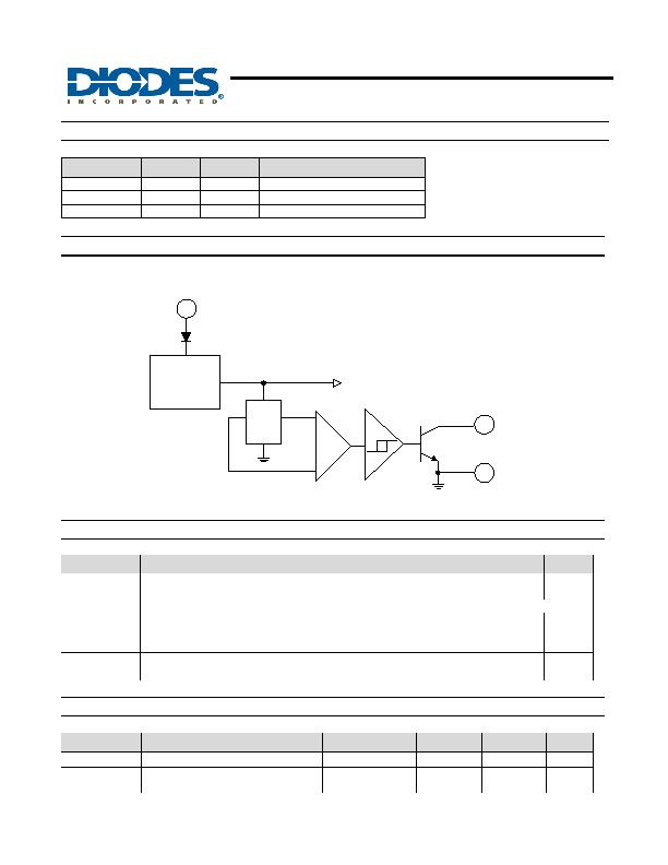
Functional Block Diagram
Regulator
Hall
plate
Amp
2
GND
DO
3
2
Vcc
1
Absolute Maximum Ratings (T
A
= 25?/SPAN>C)
Symbol
Characteristics
Rating
Unit
V
CC
Supply Voltage
20
V
V
RCC
Reverse V
CC
Polarity Voltage
-20
V
B
Magnetic Flux Density
Unlimited
V
CE
Output OFF Voltage
30
V
P
D
Package Power Dissipation
SIP-3L
550
mW
I
C
Output
ON
Current
Continuous
25
mA
T
J MAX
Maximum Junction Temperature
150
癈
T
S
Storage Temperature Range
-65~+150
癈
Recommended Operating Conditions
Symbol
Characteristic
Conditions
Min
Max
Unit
V
CC
Supply Voltage
Operating
3.5
20
V
T
A
Operating Ambient Temperature
(Note 2)
Operating
-20
85
癈
Notes: 2. Shall not exceed P
D
and Safety Operation Area.
发布紧急采购,3分钟左右您将得到回复。
相关PDF资料
ATS617LSGTN-T
IC HALL EFFECT GEAR SENSOR 4SIP
ATS625LSGTN-T
IC SENSOR GEAR TOOTH 4-SIP
ATS627LSGTN-T
IC HALL EFFECT GEAR SENSOR 4-SIP
ATS635LSETN-T
IC SENSOR GEAR TOOTH 4-SIP
ATS643LSHTN-I2-T
IC SENSOR GEAR TOOTH 4-SIP
ATS645LSHTN-I1
IC SENSOR GEAR TOOTH 4-SIP
ATS667LSGTN-T
IC SENSOR GEAR TOOTH 4SIP
ATS674LSETN-LT-T
IC SENSOR GEAR TOOTH 4-SIP
相关代理商/技术参数
ATS177PL
功能描述:工业霍耳效应/磁性传感器 SNGL BRUSHLESS LEAD-FREE RoHS:否 制造商:Honeywell 操作类型: 操作高斯: 工作电源电压: 电流额定值: 封装 / 箱体: 输出下降时间: 工作点最小值/最大值: 安装风格: 最大工作温度: 最小工作温度: 最大输出电流: 封装:
ATS177PLA
功能描述:板机接口霍耳效应/磁性传感器 Single Brushless RoHS:否 制造商:Honeywell 类型:Bipolar Hall-Effect Digital Position Sensor 工作电源电压:3 V to 24 V 电源电流:3.5 mA 最大输出电流:20 mA 工作点最小值/最大值:5 G, 55 G 最小/最大释放点(Brp):- 55 G, - 5 G 最大工作温度:+ 150 C 安装风格:SMD/SMT 封装 / 箱体:SOT-23
ATS177-PL-A
制造商:Diodes Incorporated 功能描述:HALL EFFECT SENSOR 25MA LATCH 5V/9V/12V/15V/18V 3SIP - Bulk
ATS177-PL-A-A
功能描述:板机接口霍耳效应/磁性传感器 HALL IC SNSR LATCH 3.5V-20V 25MA RoHS:否 制造商:Honeywell 类型:Bipolar Hall-Effect Digital Position Sensor 工作电源电压:3 V to 24 V 电源电流:3.5 mA 最大输出电流:20 mA 工作点最小值/最大值:5 G, 55 G 最小/最大释放点(Brp):- 55 G, - 5 G 最大工作温度:+ 150 C 安装风格:SMD/SMT 封装 / 箱体:SOT-23
ATS177-PL-A-B
功能描述:板机接口霍耳效应/磁性传感器 HALL IC SNSR LATCH 3.5V-20V 25MA RoHS:否 制造商:Honeywell 类型:Bipolar Hall-Effect Digital Position Sensor 工作电源电压:3 V to 24 V 电源电流:3.5 mA 最大输出电流:20 mA 工作点最小值/最大值:5 G, 55 G 最小/最大释放点(Brp):- 55 G, - 5 G 最大工作温度:+ 150 C 安装风格:SMD/SMT 封装 / 箱体:SOT-23
ATS177-PL-B-A
功能描述:板机接口霍耳效应/磁性传感器 BIPOLAR LATCHING 3.5V-20V 25mA RoHS:否 制造商:Honeywell 类型:Bipolar Hall-Effect Digital Position Sensor 工作电源电压:3 V to 24 V 电源电流:3.5 mA 最大输出电流:20 mA 工作点最小值/最大值:5 G, 55 G 最小/最大释放点(Brp):- 55 G, - 5 G 最大工作温度:+ 150 C 安装风格:SMD/SMT 封装 / 箱体:SOT-23
ATS177-PL-B-B
功能描述:板机接口霍耳效应/磁性传感器 BIPOLAR LATCHNG 25mA 3.5V-20V RoHS:否 制造商:Honeywell 类型:Bipolar Hall-Effect Digital Position Sensor 工作电源电压:3 V to 24 V 电源电流:3.5 mA 最大输出电流:20 mA 工作点最小值/最大值:5 G, 55 G 最小/最大释放点(Brp):- 55 G, - 5 G 最大工作温度:+ 150 C 安装风格:SMD/SMT 封装 / 箱体:SOT-23
ATS177W
功能描述:工业霍耳效应/磁性传感器 SNGL BRUSHLESS RoHS:否 制造商:Honeywell 操作类型: 操作高斯: 工作电源电压: 电流额定值: 封装 / 箱体: 输出下降时间: 工作点最小值/最大值: 安装风格: 最大工作温度: 最小工作温度: 最大输出电流: 封装:
